Classifications of making thin films: Chemical vapor deposition (CVD) and Physica vapor deposition (PVD)
(1) CVD: Chemical vapor deposition and Atomic layer deposition
(2) PVD: Evaporation and Sputtering
• Evaporation: Used target materials vaporized through thermal resistance with E-beam
• Sputtering: used energetic ions collating with target materials to detach it.
As one of the physical vapor depositions, which doesn't react with the substrate chemically, sputter deposition accelerates argon gas in the vacuum chamber, which is ionized in the plasma. This argon gas collides with a target such that atoms of targets are scattered and eventually deposited on the substrate called a glass. Usually, sputtering deposition is used for making thin films, such as silicon wafers, solar panels, and display screens.
1. Main Mechanism of sputtering
(1) Three main components in sputterings: (Sputtering) Target, Glass, and Plasma
• Target: the materials that will be deposited on glass.
• Glass: the substrates covered by target materials
• Plasma:
1.1 Types of materials that can be used in sputtering depositions.
• Pure metal, ceramic sputtering targets, and alloy sputtering targets
1.2 Sputtering process 1: Accelerating atoms colliding to target materials
When high electric voltage is applied between a target and a substrate, the electron from the target is emitted and accelerated to the target as a free electron. This free electron collides with argon atoms, forming plasma between the target and the substrate. If the electron has enough kinetic energy to ionize argon atoms, then Argon atoms get an Ar+ ion by emitting an electron. This Ar+ ion is moving to the cathode, causing collisions between the target and the ion. As a result, the target atom is disassociated from the material.
• Inert and non-reactive gas such as Ar is used.
• Two properties that the gas used in the sputtering has to have
(1) must not react chemically with the target materials.
(2) the atomic weight should be enough that the atoms can affect the target materials.
• Ar ion should have the kinematic energy enough to break the atomic bonds of targets. To do it, the Ar should accelerate without any collision with impurities in the chamber, e.g., It should have a large mean-free path.
• The threshold energy that the target atom can be emitted via sputtering with ions
\begin{equation}
E_{threshold} = \frac{\text{Heat of Vaporization}}{\gamma(1-\gamma)}, ~~\text{where $\gamma = \frac{4M_1 M_2}{(M_1 + M_2)^2}$}
\end{equation}
1.4 Sputtering process 2: Deposition of target materials on substrates
• Sputtering rate (A): The number of monolayers per second sputtered from the surface of a target
- dependent on the following factors;
(1) the sputter yield (S), (2) the molar weight of target (M), (3) material density ($\rho$), (4) ion current density (j)
- Sputtering rate
\begin{equation}
A = \frac{MSj}{\rho N_A e}
\end{equation}
where $N_A$ is the Avogadro number and $e$ is the electron charge.
2. Types of sputtering methods
(1) Direct current (DC) diode sputtering:
• With a DC voltage of around 500-1000V, a low-pressure argon plasma occurs between a target and a substrate. Positively ionized argon atom collides with target materials.
• To ionize argon gas, the cathode (anode) is located at target materials (substrates). Thus, the positively ionized argon atom accelerates into the target (or cathode, negatively charged electrode).
• Advantages:
- Cost-efficient way of applying metal targets coatings that are electrical conductors such as gold with simple designs
• Limitation
- Only electrical conductors can be applied. That is, semiconductors could not be used in DC sputtering*.
- Low sputtering rate if a few argon ions are formed
- The substrate could be damaged due to the plasma's high temperature.
* Due to the dielectricity of semiconductors, the surface where Argon ions collide is negatively charged. Thus, even though initially Ar+ ions could reach the target, due to the Coulomb force, Ar+ ions are attached and covered to the surface negatively charged, causing the plasma to no longer be maintained.
(2) RF sputtering
• An AC voltage within the radio frequency is applied to the cathode instead of the DC voltage used in a typical DC sputtering. This AC voltage prevents charge accumulation on the surface of insulating targets, which was a problem in DC sputtering.
• Advantages of RF sputtering:
- With this RF sputtering, non-conducting materials (e.g. aluminum oxide or boron nitride) can be used.
- The substrate heats up less
- Due to the oscillating electrons, the sputtering rate at the same chamber pressure is about 10 times higher than DC sputtering **.
• Limitation:
- Relatively low coating rates
- more expensive than DC sputtering
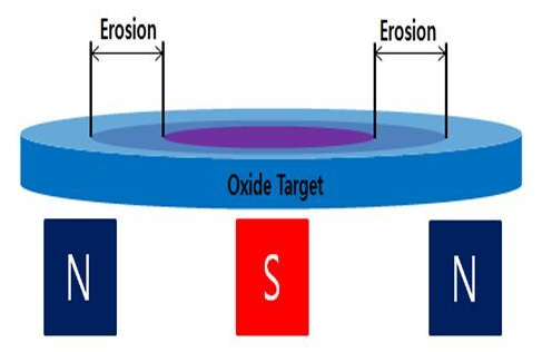
(3) Magnetron sputtering
• Magnetic field is used to control plasma bombardment of the target to increase plasma density.
• A plasma-based coating method where positively charged ions from magnetically confined plasma collide with negatively charged source materials. With a magnetic field generated by magnets behind targets, the motion of ionized atoms is accelerated further by Lorentz's force. With this strategy, magnetron sputtering can reduce the pressure required to generate plasma by ten times and increases deposition rates further.
• Advantages of magnetron sputtering: high speed, low temperature, and low damage
- High precision of film thickness and density of film coatings, which are denser than evaporations
- Perfect for metallic or insulating coatings with specific optical or electrical properties
- can be configured with multiple magnetron sources
• Limitation
- Due to the magnetic field from magnets fixed in the location, the target at the strong magnetic field can be eroded faster (called erosion), causing the target to be thrown away without using it fully.
(4) Unbalanced magnetron sputtering (UBM)
• The enhanced field coil is used to enhance the plasma density near the workplace.
• UBM can achieve a denser coating.
• The energy used in UBM is higher, causing the temperature to increase.
(5) Reactive Sputtering
• reactive gas (e.g., oxygen or nitrogen) is added to the Argon gas.
(6) Ion beam sputtering
• involves focusing an ion-electron beam on a target to sputter materials
3. Comparison between evaporation and sputtering methods
| Evaporation Method | Sputtering Methods | |
| Pros | • Permits the direct transfer of energy to the source during the heating • very efficient in depositing pur evaporated materials to the substrate • The material utilization efficiency is high relative to other methods |
• Low substrate temperature during PVD processes. - an ideal method to deposit metals for thin-film transistors • Materials that cannot be used in evaporation due to high melting points can be used in sputtering. • Typically have better adhesion on the substrate than evaporated films • Advanced processes such as epitaxial growth are possible • Better step coverage • Less radiation damage than E-beam evaporation • Easier to deposit alloys |
| Cons | • Poor step coverage • forming alloys could be difficult <Thermal resistive evaporation> • Highest impurity levels • Limited scalability • Low-density film quality • Moderate film stress • Poor uniformity without masks <E-beam evaporation> • Moderate system complexity • Moderate stress resistance • Limited scalability at reduced deposition rates and utilization • Moderate costs |
<Magnetron sputtering> • Low directionality • High costs • High system complexity • poor deposition rates for dielectrics • substrate heating, especially when dealing with energetic target materials <Ion beam sputtering> • High stress • Low scalability • Low deposition rates • High complex and costly • Slowest deposition method |
References
[1] https://www.sputtertargets.net/blog/an-overview-of-sputtering-deposition.html
[2] https://www.dentonvacuum.com/weighing-the-benefits-of-sputtering-vs-evaporation/
[3] https://www.dentonvacuum.com/pvd-magnetron-sputtering-evaporation/
[4] https://techbullion.com/whats-the-difference-between-sputtering-and-evaporation/
[5] https://alan.ece.gatech.edu/ECE6450/Lectures/ECE6450L12-Physical%20Deposition.pdf
'과학 (Science) > 실험과 관련된 것들' 카테고리의 다른 글
| [화학물질] 톨루엔 (Toluen), 벤진 (Benzene), (0) | 2024.11.09 |
|---|---|
| [실험] 화학 기구들 영어이름 (0) | 2024.08.14 |
| [실험] The BET method/Theory (0) | 2024.01.03 |
| [Materials] GE varnish (0) | 2023.07.07 |
| [materials] BeCu (0) | 2023.06.16 |
댓글